微源半导体 LP3982-18JS5 SC-70 300mA、超低噪声、小封装、超快CMOS LDO稳压器
General Description
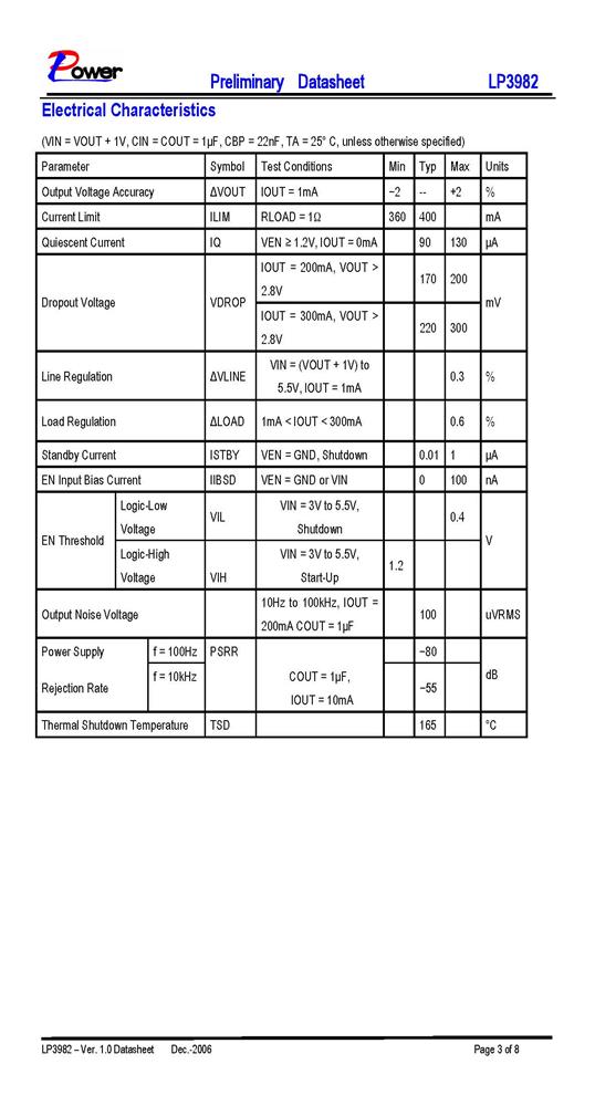
The The LP3982-18JS5 is designed for portable RF and wireless applications with demanding performance and space requirements. The LP3982-18JS5 performance is optimized for battery-powered systems to deliver ultra low noise and low quiescent current. A noise bypass pin is available for further reduction of output noise. Regulator ground current increases only slightly in dropout, further prolonging the battery life. The LP3982 also works with low-ESR ceramic capacitors, reducing the amount of board space necessary for power applications, critical in hand-held wireless devices. The LP3982 consumes less than 0.01μA in shutdown mode and has fast turn-on time less than 50μs. The other features include ultra low dropout voltage, high output accuracy, current limiting protection, and high ripple rejection ratio. Available in the 5-lead of SC-70 packages.
Absolute Maximum Ratings
◆ Supply Input Voltage: 6V
Power Dissipation, PD @ TA = 25°C
◆ SC-70: 400mW
Package Thermal Resistance
◆ SC-70, θJA: -250°C/W
◆ Lead Temperature (Soldering, 10 sec.): 260°C
◆ Storage Temperature Range: -65°C to 150°C
ESD Susceptibility
◆ HBM (Human Body Mode): 2kV
◆ MM(Machine-Mode): 200V
Recommended Operating Conditions
◆ Supply Input Voltage: 2.5V to 5.5V
◆ EN Input Voltage: 0V to 5.5V
◆ Operation Junction Temperature Range: -40°C to 125°C
◆ Operation Ambient Temperature Range: -40°C to 85°C
LP3982-18JS5产品规格书(部分)

